
Description
ZOMBIE COMPONENTS
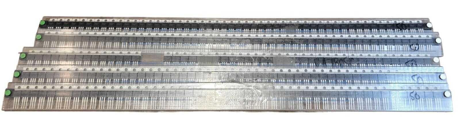
LOT OF 240 TEXAS INSTRUMENTS UA7805C Linear Voltage Regulator
3-Terminal Regulators Output Current 1.5 A Internal Thermal-Overload Protection
High Power-Dissipation Capability Internal Short-Circuit Current Limiting Output Transistor Safe-Area Compensation
This series of fixed-voltage integrated-circuit voltage regulators is designed for a wide range of applications. These applications include on-card regulation for elimination of noise and distribution problems associated with single-point regulation. Each of these regulators can deliver A of output current. The internal current-limiting and thermal-shutdown features of these regulators essentially make them immune to overload. In addition to use as fixed-voltage regulators, these devices can be used with external components to obtain adjustable output voltages and currents, and also can be used as the power-pass element in precision regulators. ORDERING INFORMATION
TJ VO(NOM) (V) PACKAGE POWER-FLEX (KTE) 5 TO-220 (KC) TO-220, short shoulder (KCS) POWER-FLEX (KTE) 8 TO-220 (KC) TO-220, short shoulder (KCS) 125°C 12 POWER-FLEX (KTE) TO-220 (KC) POWER-FLEX (KTE) TO-220 (KC) TO-220, short shoulder (KCS) POWER-FLEX (KTE) 15 TO-220 (KC) TO-220, short shoulder (KCS) 24 POWER-FLEX (KTE) TO-220 (KC) Reel of 2000 Tube of 50 Tube of 20 Reel of 2000 Tube of 50 Tube of 20 Reel of 2000 Tube of 50 Reel of 2000 Tube of 50 Tube of 20 Reel of 2000 Tube of 50 Tube of 20 Reel of 2000 Tube of 50 ORDERABLE PART NUMBER µA7824CKTER µA7824CKC TOP-SIDE MARKING µA7815C µA7824C
µA7824C Package drawings, standard packing quantities, thermal data, symbolization, and PCB design guidelines are available at ti.
Please be aware that an important notice concerning availability, standard warranty, and use in critical applications of Texas Instruments semiconductor products and disclaimers thereto appears at the end of this data sheet.
PRODUCTION DATA information is current as of publication date. Products conform to specifications per the terms of Texas Instruments standard warranty. Production processing does not necessarily include testing of all parameters.
absolute maximum ratings over virtual junction temperature range (unless otherwise noted)
Input voltage, VI: 40 V All others. 35 V Package thermal impedance, JA (see Notes 1 and 2): KC/KCS package. 25°C/W KTE package. 23°C/W Operating virtual junction temperature, TJ. 150°C Lead temperature mm (1/16 inch) from case for 10 seconds. 260°C Storage temperature range, Tstg. to 150°C
Stresses beyond those listed under “absolute maximum ratings” may cause permanent damage to the device. These are stress ratings only, and functional operation of the device at these or any other conditions beyond those indicated under “recommended operating conditions” is not implied. Exposure to absolute-maximum-rated conditions for extended periods may affect device reliability. NOTES: 1. Maximum power dissipation is a function of TJ(max), JA, and TA. The maximum allowable power dissipation at any allowable ambient temperature PD = (TJ(max) TA)/JA. Selecting the maximum of 150°C can affect reliability. 2. The package thermal impedance is calculated in accordance with JESD 51-5.
MIN µA7808C VI Input voltage IO TJ Output current Operating virtual junction temperature µA7800C series MAX °C V UNIT
electrical characteristics at specified virtual junction temperature, 500 mA (unless otherwise noted)
PARAMETER Output voltage Input voltage regulation Ripple rejection Output voltage regulation Output resistance Temperature coefficient of output voltage Output noise voltage Dropout voltage Bias current Bias current change Short-circuit output current Peak output current 1 A TEST CONDITIONS = 1 kHz to 100 kHz 62 µA7805C MIN TYP 5 MAX UNIT dB mV mV/°C V mA
A Pulse-testing techniques maintain the junction temperature as close to the ambient temperature as possible. Thermal effects must be taken into account separately. All characteristics are measured with a 0.33-µF capacitor across the input and a 0.1-µF capacitor across the output.
electrical characteristics at specified virtual junction temperature, 500 mA (unless otherwise noted)
PARAMETER Output voltage Input voltage regulation Ripple rejection Output voltage regulation Output resistance Temperature coefficient of output voltage Output noise voltage Dropout voltage Bias current Bias current change Short-circuit output current Peak output current 1 A TEST CONDITIONS = 1 kHz to 100 kHz 55 µA7808C MIN TYP 8 MAX UNIT dB mV mV/°C V mA
WE SHIP WORLD WIDE!
Additional information
| Weight | 3 lbs |
|---|---|
| Dimensions | 24.00 × 8.00 × 6.00 in |
| Brand | |
| TYPE | Linear Regulator |
| MPN | |
| Condition |
Reviews (0)
Only logged in customers who have purchased this product may leave a review.
Related products

Power Regulators & Converters
94 EA GE Critical Power Convert DC/Dc 0.75 5.5v @ 3A Sip CC109101268, Axa003a0xz
Reviews
There are no reviews yet.